- 您现在的位置:买卖IC网 > Sheet目录512 > SI5943DU-T1-GE3 (Vishay Siliconix)MOSFET DUAL P-CH 12V 6A 8PWRPAK
�� �
�
�Si5943DU�
�Vishay� Siliconix�
�Dual� P-Channel� 12-V� (D-S)� MOSFET�
�PRODUCT� SUMMARY�
�FEATURES�
�V� DS� (V)�
�R� DS(on)� (� Ω� )�
�I� D� (A)� a�
�Q� g� (Typ.)�
�?� Halogen-free�
�?� TrenchFET� ?� Power� MOSFET�
�-� 12�
�0.064� at� V� GS� =� -� 4.5� V�
�0.089� at� V� GS� =� -� 2.5� V�
�0.120� at� V� GS� =� -� 1.8� V�
�-� 6� a�
�-� 6� a�
�a�
�-6�
�6� nC�
�?� New� Thermally� Enhanced� PowerPAK� ?�
�ChipFET� ?� Package�
�-� Small� Footprint� Area�
�-� Low� On-Resistance�
�RoHS�
�COMPLIANT�
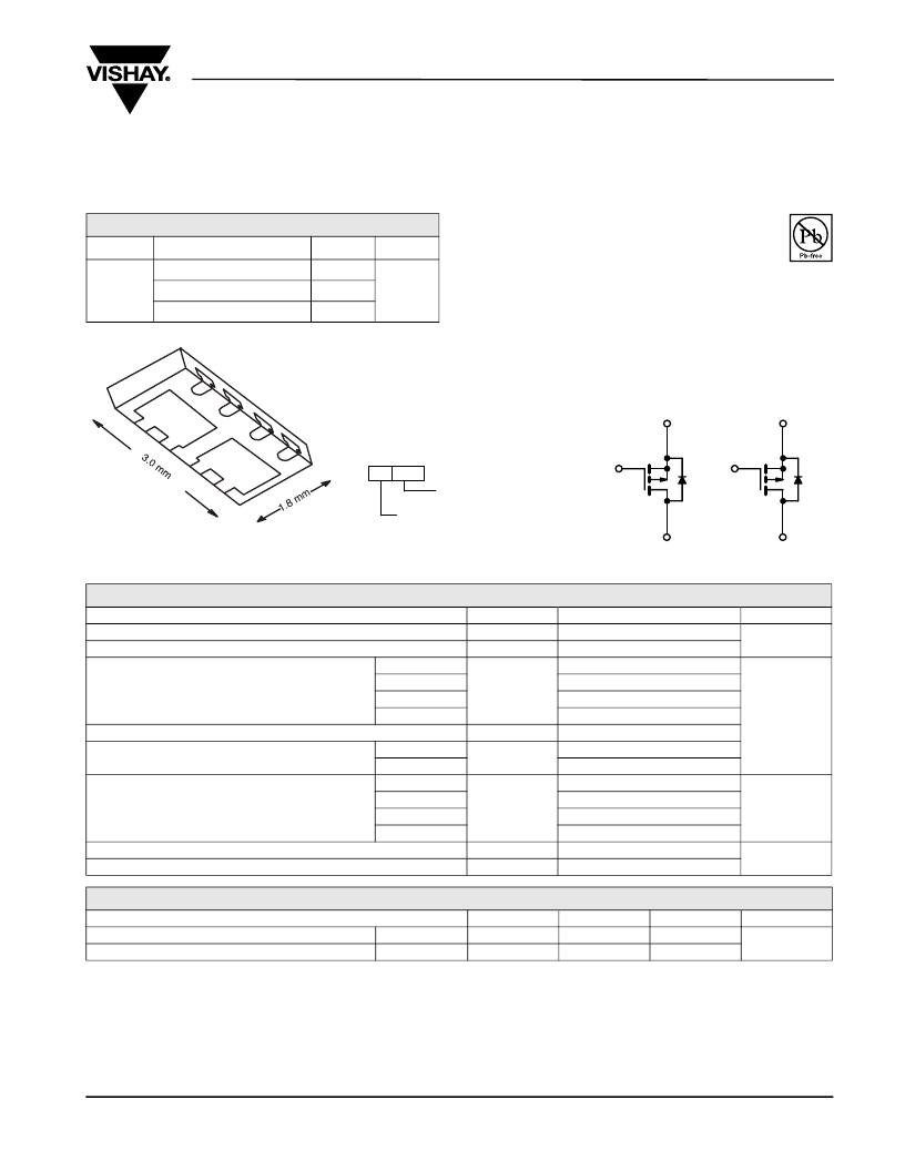
�PowerPAK� ChipFET� Dual�
�1�
�-� Thin� 0.8� mm� Profile�
�APPLICATIONS�
�8�
�D� 1�
�D� 1�
�S� 1�
�G� 1�
�2�
�S� 2�
�3�
�4�
�?� Load� Switch,� PA� Switch,� and� Charger� Switch� for� Portable�
�Devices�
�S� 1� S� 2�
�7�
�6�
�D� 2�
�5�
�D� 2�
�G� 2�
�Marking� Code�
�DC� XXX�
�Lot� Tracea� b� ility�
�and� Date� Code�
�G� 1�
�G� 2�
�Part� #�
�Code�
�Bottom� V� ie� w�
�Orderin� g� Information:� Si5943DU-T1-GE3� (Lead� (P� b� )-free� and� Halogen-free)�
�ABSOLUTE� MAXIMUM� RATINGS� T� A� =� 25� °C,� unless� otherwise� noted�
�D� 1�
�P-Channel� MOSFET�
�D� 2�
�P-Channel� MOSFET�
�Parameter�
�Drain-Source� Voltage�
�Gate-Source� Voltage�
�T� C� =� 25� °C�
�Symbol�
�V� DS�
�V� GS�
�Limit�
�-� 12�
�±8�
�-� 6� a�
�Unit�
�V�
�Continuous� Drain� Current� (T� J� =� 150� °C)�
�Pulsed� Drain� Current�
�Continuous� Source-Drain� Diode� Current�
�T� C� =� 70� °C�
�T� A� =� 25� °C�
�T� A� =� 70� °C�
�T� C� =� 25� °C�
�T� A� =� 25� °C�
�T� C� =� 25� °C�
�I� D�
�I� DM�
�I� S�
�-� 6� a�
�-� 5� b,� c�
�-� 4� b,� c�
�-� 20�
�-� 6.9�
�-� 1.9� b,� c�
�8.3�
�A�
�Maximum� Power� Dissipation�
�T� C� =� 70� °C�
�T� A� =� 25� °C�
�P� D�
�5.3�
�2.3� b,� c�
�W�
�T� A� =� 70� °C�
�1.5� b,� c�
�Operating� Junction� and� Storage� Temperature� Range�
�Soldering� Recommendations� (Peak� Temperature)� d,� e�
�T� J� ,� T� stg�
�-� 55� to� 150�
�260�
�°C�
�THERMAL� RESISTANCE� RATINGS�
�Parameter�
�Symbol�
�Typical�
�Maximum�
�Unit�
�Maximum� Junction-to-Ambient� b,� f� t� ≤� 5s�
�Maximum� Junction-to-Case� (Drain)� Steady� State�
�R� thJA�
�R� thJC�
�45� 55�
�12� 15�
�°C/W�
�Notes:�
�a.� Package� limited.�
�b.� Surface� Mounted� on� 1"� x� 1"� FR4� board.�
�c.� t� =� 5� s.�
�d.� See� Solder� Profile� (� http://www.vishay.com/ppg?73257� ).� The� PowerPAK� ChipFET� is� a� leadless� package.� The� end� of� the� lead� terminal� is� exposed�
�copper� (not� plated)� as� a� result� of� the� singulation� process� in� manufacturing.� A� solder� fillet� at� the� exposed� copper� tip� cannot� be� guaranteed� and�
�is� not� required� to� ensure� adequate� bottom� side� solder� interconnection.�
�e.� Rework� Conditions:� manual� soldering� with� a� soldering� iron� is� not� recommended� for� leadless� components.�
�f.� Maximum� under� Steady� State� conditions� is� 105� °C/W.�
�Document� Number:� 73669�
�S-81449-Rev.� B,� 23-Jun-08�
�www.vishay.com�
�1�
�发布紧急采购,3分钟左右您将得到回复。
相关PDF资料
SI5975DC-T1-GE3
MOSFET 2P-CH 12V 3.1A CHIPFET
SI5980DU-T1-GE3
MOSFET N-CH 100V PPAK CHIPFET
SI6404DQ-T1-GE3
MOSFET N-CH 30V 8.6A 8TSSOP
SI6413DQ-T1-E3
MOSFET P-CH 20V 7.2A 8TSSOP
SI6423DQ-T1-GE3
MOSFET P-CH 12V 8.2A 8-TSSOP
SI6466ADQ-T1-GE3
MOSFET N-CH 20V 6.8A 8TSSOP
SI6467BDQ-T1-GE3
MOSFET P-CH 12V 6.8A 8TSSOP
SI6924AEDQ-T1-GE3
MOSFET N-CH 28V ESD 8-TSSOP
相关代理商/技术参数
SI5944DU
制造商:VISHAY 制造商全称:Vishay Siliconix 功能描述:Dual N-Channel 40-V (D-S) MOSFET
SI5944DU-T1-E3
功能描述:MOSFET 40V 6.0A 10W RoHS:否 制造商:STMicroelectronics 晶体管极性:N-Channel 汲极/源极击穿电压:650 V 闸/源击穿电压:25 V 漏极连续电流:130 A 电阻汲极/源极 RDS(导通):0.014 Ohms 配置:Single 最大工作温度: 安装风格:Through Hole 封装 / 箱体:Max247 封装:Tube
SI5944DU-T1-GE3
功能描述:MOSFET 40V 6.0A 10W 112mohm @ 10V RoHS:否 制造商:STMicroelectronics 晶体管极性:N-Channel 汲极/源极击穿电压:650 V 闸/源击穿电压:25 V 漏极连续电流:130 A 电阻汲极/源极 RDS(导通):0.014 Ohms 配置:Single 最大工作温度: 安装风格:Through Hole 封装 / 箱体:Max247 封装:Tube
SI5945DU
制造商:VISHAY 制造商全称:Vishay Siliconix 功能描述:Dual P-Channel 20-V (D-S) MOSFET
SI5947DU-T1-E3
功能描述:MOSFET DUAL P-CH 20V(D-S) RoHS:否 制造商:STMicroelectronics 晶体管极性:N-Channel 汲极/源极击穿电压:650 V 闸/源击穿电压:25 V 漏极连续电流:130 A 电阻汲极/源极 RDS(导通):0.014 Ohms 配置:Single 最大工作温度: 安装风格:Through Hole 封装 / 箱体:Max247 封装:Tube
SI5947DU-T1-GE3
功能描述:MOSFET 20V 6.0A 10.4W RoHS:否 制造商:STMicroelectronics 晶体管极性:N-Channel 汲极/源极击穿电压:650 V 闸/源击穿电压:25 V 漏极连续电流:130 A 电阻汲极/源极 RDS(导通):0.014 Ohms 配置:Single 最大工作温度: 安装风格:Through Hole 封装 / 箱体:Max247 封装:Tube
SI595SA500M000DGR
制造商:Silicon Laboratories Inc 功能描述:
SI5975DC
制造商:VISHAY 制造商全称:Vishay Siliconix 功能描述:Dual P-Channel 12-V (D-S) MOSFET